
Pick up any electronic device and you’ll notice what’s on the outside — the screen, the buttons, the finish. What you won’t notice is the engineering that went into every internal component keeping that device alive. The connectors that carry current without melting. The housings that protect sensitive circuitry from heat and moisture. The structural parts that don’t flex or creep under sustained mechanical load. These aren’t accidents of design. They’re the result of deliberate manufacturing choices, and one process quietly responsible for many of them is compression molding.
It doesn’t make headlines the way new display technologies or chip architectures do. But in the world of electronics manufacturing, it solves problems that other processes simply can’t, and understanding why matters for engineers, product designers, and anyone curious about how the devices around them are actually built.
Read More: IT CONSULTING IN SAN DIEGO: EMPOWERING BUSINESSES T O THRIVE IN A DIGITAL WORLD
Why Compression Molding Fits the Demands of Modern Electronics
Electronics impose brutal requirements on the materials inside them. Components need to handle heat generated during operation without softening or warping. They need to resist electrical conductivity to protect circuits and users alike. They need dimensional stability — a part that shifts even slightly under thermal cycling can break a connection, crack a seal, or misalign an assembly.
Thermoset polymers, which are the core material category used in this process, meet those requirements in ways thermoplastics often can’t. Once cured, a thermoset forms a permanent cross-linked molecular structure. It doesn’t soften when temperatures rise. It doesn’t absorb moisture the way some engineering plastics do. And because it’s inherently a poor electrical conductor, it performs reliably in applications where insulation is critical.
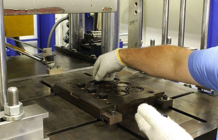
This is why you’ll find components made through this process throughout electrical distribution systems, power connectors, relay housings, and motor end caps — anywhere heat and electricity coexist and the tolerance for material failure is zero. The process applies heat and pressure together to cure the material inside a precisely shaped mold, which means parts come out dimensionally accurate and mechanically consistent, batch after batch.
For product designers working on devices where these properties matter, www.nicerapid.com is a useful resource for exploring prototyping and custom manufacturing options early in development, before committing to tooling.
Smaller Devices, Bigger Demands — Applications Across the Tech World
The scale of electronics has shrunk dramatically over the past few decades, but the performance expectations have only climbed. Wearables, for example, sit against skin, face perspiration, body heat, and constant mechanical movement. The enclosures and structural components inside need to hold their shape over years of daily wear. Certain rubber and silicone formulations processed through matched-die tooling can deliver that kind of resilience in compact, precise geometries that suit small-form-factor device design.
In industrial and commercial electronics — think control panels, programmable logic controllers, and power management units — the internal switching components and terminal insulation blocks are often produced this way. The heat resistance of cured thermosets is particularly valuable here because these devices can run continuously for years in environments where ambient temperatures are not controlled.
Telecommunications infrastructure is another area where this manufacturing approach earns its keep. Antenna mounts, cable management components, and junction box housings need to perform outdoors across a wide temperature range without cracking, expanding, or conducting electricity. Phenolic and melamine-based materials processed under heat and pressure deliver that combination of properties with a consistency that’s hard to achieve through other means.
Even within consumer electronics assembly, small insulating bushings, board standoffs, and protective shields rely on the same logic — stable material, accurate geometry, predictable performance
What Engineers Get Right and What Trips Them Up
Designing for this process requires a mindset shift if you’re coming from thermoplastic injection molding. The upside is real: lower tooling cost, excellent surface finish on flat or gently contoured parts, and no sink marks caused by cooling shrinkage, which is a persistent headache in thermoplastic design.
The adjustment is in geometry. Deep undercuts, very thin walls below a certain threshold, and highly complex internal cavities push against what this process handles cleanly. The material flows under compression rather than injection pressure, which means the design needs to accommodate that. Draft angles matter. Wall thickness uniformity matters. Parting line placement matters.
Getting those details right early — ideally during prototype evaluation rather than after production tooling has been cut — saves significant time and money. It’s the kind of decision that doesn’t show up in a product review but shapes whether a device lasts three years or ten.
What Compression Molding Means for the Future of Tech Manufacturing
The ongoing push toward more durable, heat-resistant, and electrically reliable electronics is actually creating renewed interest in this process rather than reducing it. As devices run hotter, operate in more demanding environments, and face longer expected service lives, the material limitations of standard thermoplastics become harder to engineer around.
Compression molding offers something that modern manufacturing increasingly needs: a reliable path to high-performance thermoset parts without the tooling overhead of more complex processes. Composite materials — including glass-fiber and carbon-fiber reinforced grades — can be processed this way to produce structural components with mechanical properties that aluminum or standard plastics can’t match at the same weight.
That’s not a niche proposition. As product categories from electric vehicles to ruggedized field electronics continue to grow, the demand for components that handle heat, maintain structural integrity, and resist electrical failure will only expand. The process isn’t new, but the problems it solves are very much part of where technology is heading.
Read More: COMMON AREAS WHERE HOTEL MANAGEMENT MAKES MISTAKES
The devices of the future will look different from the ones we use today. But inside them, the same fundamental manufacturing logic will apply — match the right material to the right process, design thoughtfully, and build parts that don’t fail quietly when it matters most.